
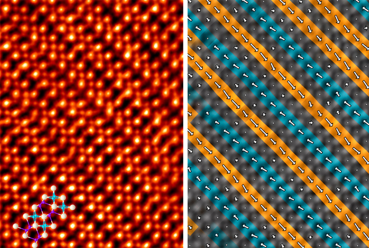
Harnessing atomic structure to advance semiconductor technology
Researchers at Washington University in St Louis have developed a novel method to manipulate atomic structures within semiconductor materials.
The story
in brief.
What happened, who it affects, and why it landed on our intelligence desk — in plain English, sixty seconds or less.
Researchers at Washington University in St Louis have developed a novel method to manipulate atomic structures within semiconductor materials. This breakthrough allows for precise control over electronic properties at the nanoscale, potentially overcoming current physical limitations in chip miniaturisation. The study demonstrates how altering atomic arrangements can significantly enhance device performance and energy efficiency. This advancement addresses critical bottlenecks in modern electronics manufacturing, offering a pathway to more powerful and sustainable computing hardware. The findings suggest a shift towards atomic-level engineering in semiconductor design, moving beyond traditional lithography constraints to optimise material behaviour from the ground up for next-generation technological applications.
Indicative index of skill mentions in professional job postings for the field this story moves (2019 = 1)
What this means
for your career.
Every headline redistributes opportunity. Here is who this one rewards — and how to be on the right side of it.
This development signals a shift towards atomic-level precision in hardware engineering, elevating the value of materials science and quantum physics expertise. If you work in semiconductor manufacturing or hardware R&D, you must now understand nanoscale material behaviour. Traditional electronics knowledge is no longer sufficient; you need to grasp how atomic structures dictate device performance. Professionals in engineering and innovation should prioritise upskilling in advanced materials characterisation and quantum mechanics. A smart move is to integrate these insights into your current projects, focusing on efficiency gains and new material applications. Engage with cross-functional teams bridging physics and engineering to stay ahead. This is not just theoretical; it will reshape product development cycles and require a deeper technical foundation than ever before.
For this story, the fields that convert it into pay are Engineering, Innovation, AI in Engineering and Data analytics — exactly the programmes matched below. The chart shows the indicative salary uplift certified professionals report in each of those fields; every one of them is a click away, from £79, finishing in as few as 20 days.
Indicative ranges from published continuing-education salary studies, by field — each field is a recommended course below
Enrol in these
to benefit.
These programmes position you for exactly this shift — online, self-paced, and finishing with a verifiable certificate you can share the day you pass.
 Best match
Certificate in Engineering
 Recommended
Certificate in Innovation
 Recommended
Certificate in AI in Engineering
 Recommended
Certificate in Data analytics
Launch pricing shown against standard certificate value. The fee you see today is the fee you lock in.
This briefing is based on reporting by WashU on 5 Nov, 22:03. Read the original coverage →
Read the news. Then outrun it.
Every LSBR programme is online, self-paced and from £79 — so a headline today can be your credential this month.
